How direct-view LED works, from a single diode to the processor behind a video wall.
19 articles · 7 sections
LEDs
Light Emitting Diodes (LED)
A Light Emitting Diode (LED) is a semiconductor device that produces light when electrical current passes through it. LEDs are the foundational building block of modern direct-view LED (dvLED) displays, and understanding how they work explains why dvLED performs differently from every other display technology.
Quick reference
Term
Definition
LED
A semiconductor device that emits light when current passes through it
Die (Chip)
The semiconductor material inside an LED where light is generated
P-type Layer
The positive semiconductor layer, containing electron "holes"
N-type Layer
The negative semiconductor layer, containing free electrons
Photon
A subatomic particle of light, released when an electron crosses the P-N junction
Reflector Cup
A small housing that encapsulates the RGB dies and directs light outward
Anode
The positive electrical terminal of an LED
Cathode
The negative electrical terminal of an LED
How an LED chip Works
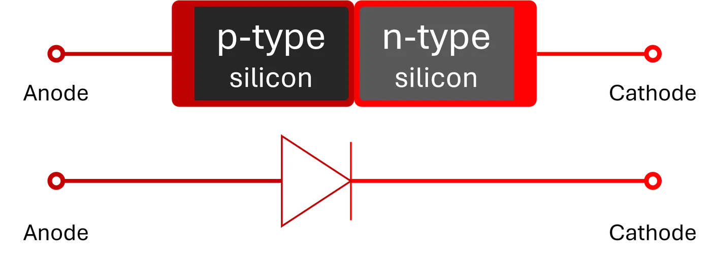
An LED is built from layers of semiconductor material — typically gallium nitride — engineered with impurities to create two distinct regions:
P-type Layer: Contains an abundance of "holes" (positive charge carriers)
N-type Layer: Contains an abundance of electrons (negative charge carriers)
When current is applied, electrons from the N-type layer are pushed across the junction into the P-type layer, where they fall into holes and release energy as photons — light. The color of that light is determined by the semiconductor material and its energy gap, which is covered in detail in LED Chip Fabrication.
Key Components of an LED chip
The Die (Chip): The semiconductor material at the core of every LED, where light is actually generated. A single RGB pixel contains three dies — one red, one green, one blue.
Reflector Cup: A small housing that holds the three dies and is shaped to direct light outward toward the viewer.
Anode (+): The positive electrical terminal through which current enters the LED.
Cathode (-): The negative electrical terminal through which current exits. How the cathode and anode are configured across a display has significant implications for power efficiency.
A Brief History: From Backlight to Direct View
The term "LED display" has meant different things at different times, and the distinction matters.
For most consumers, "LED TV" refers to a liquid crystal display (LCD) that uses LEDs as a backlight — replacing the older cold cathode fluorescent lamp (CCFL) technology. The LEDs in these screens never form the image directly; they simply illuminate it from behind. This is what might be called consumer LED.
Commercial LED, or direct-view LED (dvLED), works fundamentally differently. The LEDs themselves are the image. There is no LCD layer, no backlight — each pixel is an independently controlled light source. This allows for dramatically higher brightness, wider viewing angles, and displays of virtually any size or shape.
The "dv" in dvLED exists specifically to draw that line — distinguishing professional direct-view technology from the consumer LCD panels that borrowed the LED name.
LED Pixel Packaging
In a dvLED display, LEDs are packaged and mounted onto a Printed Circuit Board (PCB) in several different ways — including Surface Mount Device (SMD), Chip-on-Board (COB), and Micro-in-Package (MIP), among others. Each approach has distinct implications for pixel density, durability, repairability, and cost. These technologies are covered individually in the Pixels section of this encyclopedia.
LEDs
LED Chip Fabrication
Before an LED can be mounted onto a display, it must first be manufactured at a microscopic scale. This article covers the process of fabricating an individual LED chip — from raw semiconductor wafer to a finished, mountable package — a process that underlies all dvLED pixel technologies.
Quick reference
Term
Definition
Wafer
A thin disc of semiconductor material from which LED chips are cut
Epi-Wafer
A wafer with semiconductor layers grown on it that determine LED color and efficiency
Die (chip)
An individual microscopic LED chip cut from a wafer
Lead Frame
The metal skeleton of an LED package that connects the die to the outside world
Reflector Cup
A recessed cavity in the lead frame that houses the dies and directs light outward
Wire Bonding
The process of connecting a die to the lead frame using ultra-fine gold or copper wire
Ball Bond
The connection point where a bond wire meets the die surface
Wedge Bond
The connection point where a bond wire meets the lead frame
Encapsulation
The silicone or epoxy resin coating that protects and seals the finished package
Bandgap
The energy gap in a semiconductor material that determines the wavelength — and therefore color — of emitted light
From Wafer to Die
Everything begins with a semiconductor wafer. Layers of semiconductor material — typically gallium nitride — are grown onto the wafer in a process that determines the color and efficiency of the resulting LEDs. This layered wafer is called an epi-wafer.
The key to color lies in the bandgap — a property of the semiconductor material that determines how much energy an electron releases when it crosses the P-N junction. That energy determines the wavelength of the emitted light, and wavelength determines color. By engineering the composition of the semiconductor layers during growth, manufacturers set the bandgap — and therefore the color — of each die before it is ever cut from the wafer. Red, green, and blue dies are grown separately, using different material compositions tuned to their respective wavelengths.
Patterns are then etched into the epi-wafer to define individual diode structures. The wafer is cut into thousands of microscopic pieces, each one a functional LED chip called a die.
The Lead Frame
The lead frame is the internal skeleton of an LED package. Mechanically stamped from a thin sheet of copper alloy and plated with silver or gold for reflectivity, it serves as the structural and electrical bridge between the microscopic die and the Printed Circuit Board (PCB) it will eventually be mounted on.
The lead frame features recessed cavities called reflector cups — small, bowl-shaped housings into which the dies are placed. The copper base carries the electrical signals, while the geometry of the cup is engineered to direct light outward toward the viewer.
Die Placement
A tiny droplet of conductive epoxy resin is dispensed into the bottom of each reflector cup. A high-speed pick-and-place machine then lifts individual dies and places them into the cup, aligning each one within microns of its target coordinates. In a standard RGB package, three dies are placed — one red, one green, one blue.
Wire Bonding
Once the dies are secured, they must be electrically connected to the lead frame. A robotic bonder uses ultra-fine wire — often thinner than a human hair — to connect the top contact of each die to the lead frame's bonding pads.
The bonder creates a ball bond at the die surface and a wedge bond at the lead frame, forming a conductive bridge through which current flows to produce light.
Encapsulation
With the dies placed and bonded, the reflector cups are filled and sealed with silicone or epoxy resin. The slanted walls of the cup — typically angled between 45 and 60 degrees — are designed to catch light emitting from the sides of the die and redirect it outward. This completes the finished LED package, ready for mounting.
Power
The Anode and Cathode Functions
Every LED has two electrical terminals — the anode and the cathode. These terminals control the direction of current flow through the diode, which is what makes the LED produce light. Understanding how they function is foundational to understanding how dvLED displays are powered and managed.
Quick reference
Term
Definition
Anode (+)
The positive terminal through which current enters the LED
Cathode (-)
The negative terminal through which current exits the LED
Polarity
The requirement that current flow in one specific direction for the LED to function
Forward Voltage
The minimum voltage required to push current through a specific LED color
Thermal Pad
A heat-dissipating component on the PCB connected to the cathode terminal
The Basic Anode and Cathode Functions
The anode is the positive terminal — current enters here. The cathode is the negative terminal — current exits here. Because LEDs are polarized devices, they will only produce light when current flows in this specific direction. Reverse the polarity and nothing happens.
As covered in Light Emitting Diodes (LED), when current flows correctly through the P-N junction, electrons cross the junction and release energy as photons — light.
Forward Voltage and Heat
Not all three-color dies in an RGB pixel require the same amount of voltage to operate. Each color has a characteristic forward voltage — the minimum voltage needed to drive it:
Red: lowest forward voltage (approximately 1.8–2.2V)
Green: mid-range forward voltage (approximately 2.9–3.5V)
Blue: highest forward voltage (approximately 2.9–3.5V)
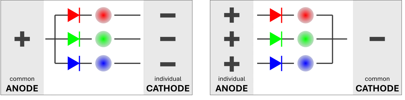
In a traditional common anode configuration, a single supply voltage — typically 5V — is sent to all three diodes simultaneously. Because red has the lowest forward voltage, it has the largest gap between what it needs and what it receives. That gap is not used productively — it is dissipated as wasted heat. Green and blue, with higher forward voltages, waste proportionally less.
This is the core inefficiency that Common Cathode technology is designed to solve, covered in detail in Common Cathode Technology.
Heat Dissipation
In dvLED applications, the cathode terminal plays an active role in thermal management. The cathode is typically connected to a thermal pad — a larger conductive surface on the PCB designed to draw heat away from the semiconductor die and spread it across the board. This prevents heat from accumulating at the chip and extends the operational lifespan of the display.
Power
Common Cathode Technology
Common Cathode technology is an energy-efficient method of powering the individual Red, Green, and Blue (RGB) diodes within a dvLED pixel. By delivering precisely matched voltages to each color, it eliminates the wasted energy inherent in traditional common anode designs — reducing heat, extending component life, and lowering operational costs.
Quick reference
Term
Definition
Common Anode
A power architecture where a single voltage is supplied to all three color diodes simultaneously
Common Cathode
A power architecture where the cathodes of all three diodes share a ground, allowing separate voltages to be supplied to each anode
Forward Voltage
The minimum voltage required to drive a specific LED color
Blue-Shift
A color distortion that occurs when LEDs overheat, causing the display to skew toward blue
How Common Cathode Works
Every RGB pixel contains three diodes — red, green, and blue. Each requires a different forward voltage to operate:
Red: 1.8 – 2.2V
Green: 2.9 – 3.5V
Blue: 2.9 – 3.5V
Common Anode (Traditional): A single supply voltage — typically 5V — is sent to the positive terminal (anode) of all three diodes simultaneously. Because red has the lowest forward voltage, it has the largest gap between what it needs and what it receives. That gap is dissipated as wasted heat. Green and blue, with higher forward voltages, waste proportionally less. As covered in The Anode and Cathode Functions, this is the fundamental inefficiency of common anode architecture.
Common Cathode: The negative terminals (cathodes) of all three diodes are tied to a shared ground. This allows the system to supply a dedicated, precisely matched voltage to each anode independently — approximately 2.2V to red and 3.2V to green and blue. There is no excess voltage to dissipate. The energy that would have become heat is simply never supplied.
A note on implementation: Common cathode is not a feature of the pixel alone. It requires a compatible handshake between a common cathode capable pixel — such as MIP — and compatible IC drivers on the PCB. Both components must support common cathode architecture for the power efficiency advantages to be realized.
Comparison between Common Anode and Cathode configurations
Feature
Common Anode
Common Cathode
Voltage Supply
Single (e.g., 5V)
Dedicated per color (~2.2V red, ~3.2V G/B)
Heat Generation
High
Low
Power Consumption
Baseline
Up to 20-30% lower
Component Lifespan
Baseline
Longer due to lower operating temperatures
Why Common Cathode Matters
Thermal management is the central engineering challenge in high-density dvLED displays. Common Cathode addresses it directly:
Reduced heat keeps the entire panel cooler, preventing the blue-shift color distortion that occurs when LEDs overheat
Higher brightness potential — with better thermal management, LEDs can be driven harder without risk of premature degradation
Lower operating costs — meaningful energy savings at scale, particularly relevant for large permanent installations
Extended reliability — lower heat reduces mechanical stress on PCB solder joints and component packaging
Power | The Anode and Cathode Functions
Pixels | Micro-In-Package (MIP)
Components | Integrated Circuits (IC Drivers)
Diode bonding
Gold and Copper Wire
Before flip-chip technology emerged, every LED die required a physical wire to complete its electrical connection to the substrate. That wire was historically gold — and for a long time, nobody questioned it. When copper arrived as an alternative, it sparked a debate that was louder than it deserved to be.
Quick reference
Term
Definition
Bond Wire
An ultra-fine wire connecting the LED die to the PCB substrate
Gold Wire
The original bonding wire material — reliable, corrosion-resistant, expensive
Copper Wire
The modern economy alternative — comparable performance at significantly lower cost
Encapsulation
The protective resin coating that seals the LED package from the environment
Corrosion
The degradation of copper wire when exposed to moisture or reactive gases
A Brief History of LED Bonding Wire
Wire bonding has been the standard method of connecting LED dies to their substrates since the technology's earliest days. Gold was the default material — it bonds reliably, resists corrosion, and was well understood by manufacturers. For decades it was simply the way things were done.
As LED manufacturing scaled up and cost pressures increased, copper emerged as a viable alternative. Copper wire is significantly cheaper than gold and performs comparably under normal conditions. Its adoption was largely manufacturer-driven, motivated by cost reduction at scale.
The Gold vs. Copper Debate
When copper wire entered the market, a vocal contingent of manufacturers and integrators pushed back — arguing that gold was the only serious choice for professional displays and that copper represented a compromise on quality.
That position doesn't hold up under scrutiny.
Copper is only a liability in one specific scenario: encapsulation failure in a corrosive environment. Copper can corrode when exposed to moisture or reactive gases — but it never sees those conditions inside an intact LED package. The encapsulation seals it completely.
What Actually Causes Pixel Failure
The dominant causes of pixel failure in dvLED displays are:
(VAST MAJORITY) Physical impact — the LED package is displaced from its solder contacts entirely
Encapsulation failure — the protective coating is compromised, exposing internals to the environment
Die failure — the semiconductor itself degrades or fails
Wire material is only relevant in the second scenario, and only when environmental conditions are also corrosive. Physical impact — the leading failure mode — happens regardless of whether the wire inside is gold or copper.
The copper corrosion argument addresses a narrow slice of an already minority failure mode.
Where Each Material Stands Today
Gold wire remains in use — not because it outperforms copper in real-world deployments, but because it is more established. Manufacturers with legacy processes built around gold have little incentive to retool.
Copper has won the economy argument. For the vast majority of installations, it delivers equivalent reliability at lower cost.
Flip-chip, covered in the following article, renders the debate largely academic for high-density applications — by eliminating bond wires entirely.
Diode bonding
Flip-Chip
Flip-Chip is a method of bonding an LED die to its substrate by flipping the chip upside down and connecting its electrodes directly to the PCB — eliminating the need for bond wires entirely. The result is a more efficient, more durable, and more compact LED construction than traditional wire-bonded approaches.
Quick reference
Term
Definition
Die
The individual LED semiconductor chip
Substrate
The surface to which the die is mounted and electrically connected
Electrode
The electrical contact point on the die (positive or negative)
Sapphire Substrate
The transparent crystalline base layer of the LED die through which light escapes
Solder Bump
A small deposit of solder paste that mechanically and electrically connects the flipped die to the PCB
Wire Bond
The traditional alternative to flip-chip — ultra-fine gold or copper wire connecting the die to the PCB
Thermal Resistance
A measure of how easily heat travels away from the die
The Structural Difference
In a traditional wire-bonded LED, the die sits face-up on the substrate. Its electrodes face upward and are connected to the PCB via ultra-fine gold or copper wires. The sapphire substrate sits at the bottom.
In a flip-chip LED, that orientation is literally inverted:
The electrodes face downward, connecting directly to PCB pads via solder paste
The sapphire substrate sits on top, acting as a transparent window through which light exits
No bond wires are used
The solder paste used in flip-chip bonding is significantly stronger than standard SMD solder — producing a mechanical and electrical connection that is both more reliable and more thermally efficient than wire bonding.
Key Advantages of Flip-chip
Light Output
In a wire-bonded die, the electrodes and bond wires sit on the top surface and physically obstruct a portion of the emitted light. With electrodes moved to the underside, the entire top surface is unobstructed — producing higher lumen output at the same power level.
Thermal Management
In a wire-bonded configuration, heat generated at the P-N junction must travel through the sapphire substrate — a poor thermal conductor — before reaching the PCB. In flip-chip, the heat-generating junction sits directly adjacent to the metal electrodes, which contact the PCB directly. This dramatically shortens the thermal path, keeping operating temperatures lower and extending display lifespan.
Reliability
A meaningful percentage of pixel failures in wire-bonded displays trace back to broken or disconnected bond wires — caused by physical impact, thermal expansion, or manufacturing stress. Eliminating the wires removes this failure point entirely, producing a more durable display particularly suited to high-traffic or interactive environments.
Pixel Density
At very fine pixel pitches, the physical space available for each LED element becomes extremely limited. Bond wires at these scales introduce risk of electrical shorts and structural instability. Flip-chip's wire-free construction allows dies to be placed much closer together, enabling the ultra-fine pitches required of MIP displays.
Comparison
Feature
Wire-Bond
Flip-Chip
Electrode Position
Top of die, facing up
Bottom of die, facing down
Electrical Connection
Gold or copper bond wires
Direct solder paste contact
Light Obstruction
Partial – wires and pads block surface
None – full substrate unobscured
Heat Dissipation
Slower – travels through sapphire substrate
Direct – junction contacts PCB immediately
Durability
Vulnerable to wire breakage
No wires to break
Module treatments
Epoxy and Protective Coatings
Once a module is assembled, it can receive one or more surface treatments that improve durability, environmental resistance, and visual performance. Traditional treatment of the module’s pixels varies based on pitch. Wider pitches, starting around 1.8mm, will often have a physical mask grid which is installed between the pixels and is secured by adhesive or screws. Finer pitches often get no physical mask as the gap is too narrow. Whether a physical installed mask or no mask, the pixels have some ability to shift from physical impact which makes that pixel lose signal and turn off. Physical impact is the leading cause of dark pixels. There are several treatments which can be applied to SMD, MIP, and IMD modules to better protect the pixels. The most significant of these is an epoxy treatment — a protective layer applied over the pixel surface that secures individual pixels against physical displacement. Additional treatments address moisture resistance and full environmental sealing for outdoor and high-exposure applications.
Epoxy treatment applies to SMD, MIP, and IMD pixel technologies. It does not apply to COB, which uses a continuous flood coat encapsulation as part of its core architecture.
Quick reference
Term
Definition
Epoxy Coat
A thick epoxy infill that covers pixels with a mostly smooth, flat surface — commonly but misleadingly called "GOB"
Epoxy Mask
A thinner epoxy infill treatment as compared to Epoxy Coat. Epoxy Mask preserves the pixel surface texture, conceals module seams and repaired pixels more effectively
GOB
Industry term for Epoxy Coat (Glue-On-Board) — widely misused as if it were a pixel technology rather than a surface treatment
HOB / hGOB / sGOB
Industry terms for Epoxy Mask variants — Half-On-Board, Half-Glue-On-Board, Shrink-Glue-On-Board
Hydrophobic Coating
A moisture-resistant treatment applied to the module rear to protect internal components from humidity and water ingress
IP Rating
Ingress Protection rating — a standardized measure of a display's resistance to dust and moisture
A Note on Industry Terminology
LED technology is being pioneered and advancing organically, producing several terms which aren’t standardized. ‘microLED’ and ‘miniLED’ are included in this group, having names which people recognize but no standard and ubiquitous definition. When it regards epoxy protective treatments, the industry has done itself no favors. "GOB" — Glue-On-Board — has left many integrators and end users to think epoxy was a pixel technology rather than a surface treatment applied to existing pixels. Terms like HOB, hGOB, and sGOB followed, each attempting to describe a thinner variant with its own acronym.
Vanguard LED uses two terms: Epoxy Mask and Epoxy Coat. They describe what the treatment actually does. Everything else in this article uses those terms.
Why Epoxy Matters
Physical impact is the leading cause of pixel failure in LED displays — specifically, pixels being displaced from their solder contacts by shock or vibration. Epoxy treatment addresses this directly by bonding the pixel surface to the module, dramatically reducing the risk of displacement from impact.
A secondary benefit is thermal — epoxy conducts heat away from the pixel surface, supplementing the thermal management already performed by the module PCB.
Epoxy Coat
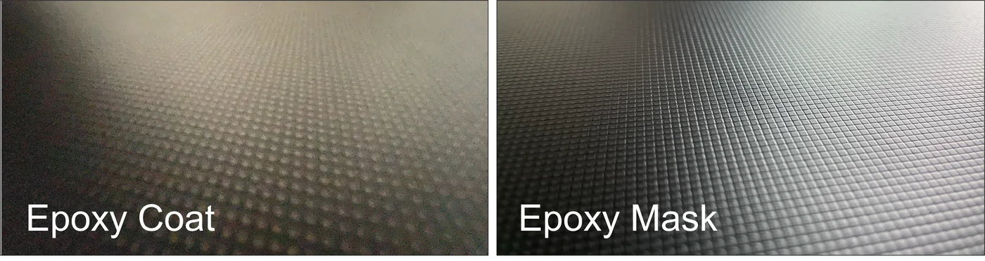
Epoxy Coat is a thick epoxy infill applied across the pixel surface, filling the space between pixels and leaving a mostly smooth, flat top surface. The result is a module that looks and feels more like a solid slab than an array of individual components.
Advantages:
Strong pixel securing from physical impact
Smooth surface is easy to clean
Repairable — damaged areas can serviced then filled with replacement epoxy
Limitations:
The smooth, flat surface reflects ambient and natural light uniformly, which can produce glare and reduce perceived contrast in real-world lighting conditions
Module seams are highly visible under ambient light — the smooth surface offers nothing to break up or conceal the gap between adjacent modules
Epoxy Coat repair, while possible, leaves a more apparent patch than Epoxy Mask repair due to the smooth surface requiring a seamless fill match
Epoxy Mask
Epoxy Mask uses less epoxy than Epoxy Coat, applied in a way that preserves the natural texture of the pixel surface rather than smoothing over it. The individual pixel profile remains visible and tactile.
This is Vanguard's recommended treatment, and the reasons are both functional and visual.
Advantages:
The preserved surface texture actively breaks up and diffuses ambient and natural light, reducing glare and improving perceived contrast in real-world lighting conditions
Module seams are far less visible under the textured surface — the irregular profile conceals transitions between modules significantly better than a smooth coat
Repair is cleaner and easier to conceal — the textured surface masks minor variations in the repair material far more effectively than a smooth coat
Looks substantially better in practice across the range of real-world lighting environments displays actually operate in
Limitations:
Slightly less pixel securing coverage than Epoxy Coat due to reduced epoxy volume — though still a significant improvement over untreated modules
Moisture and Environmental Treatments
Hydrophobic Coating
A hydrophobic treatment applied to the rear of the module protects internal components and PCB traces from humidity and moisture ingress. This is standard practice for displays in environments with elevated humidity, and a baseline recommendation for any permanent outdoor-adjacent installation.
Full Waterproofing — IP65 and Above
For displays requiring full environmental sealing — outdoor installations, high-wash environments, or applications requiring a certified IP rating — a comprehensive waterproofing treatment is applied around the pixel surface in addition to the rear coating. This seals the module against direct water exposure, qualifying it for IP65 and higher ratings.
IP65 certification indicates complete dust protection and resistance to low-pressure water jets from any direction — the standard threshold for outdoor dvLED installations.
Repair
All epoxy-treated modules follow the same field repair workflow as untreated modules — module swap from onsite spares, with the pulled module sent offsite for repair. The epoxy treatment affects the ease and visibility of the offsite repair itself:
Epoxy Mask — repair is the cleanest of any surface treatment. The textured surface naturally conceals minor variations in the repair material, making treated repairs nearly undetectable.
Epoxy Coat — repair is possible but more apparent. The smooth surface requires a precise match of the replacement epoxy to avoid a visible patch.
Pixels
Surface-Mount-Device (SMD)
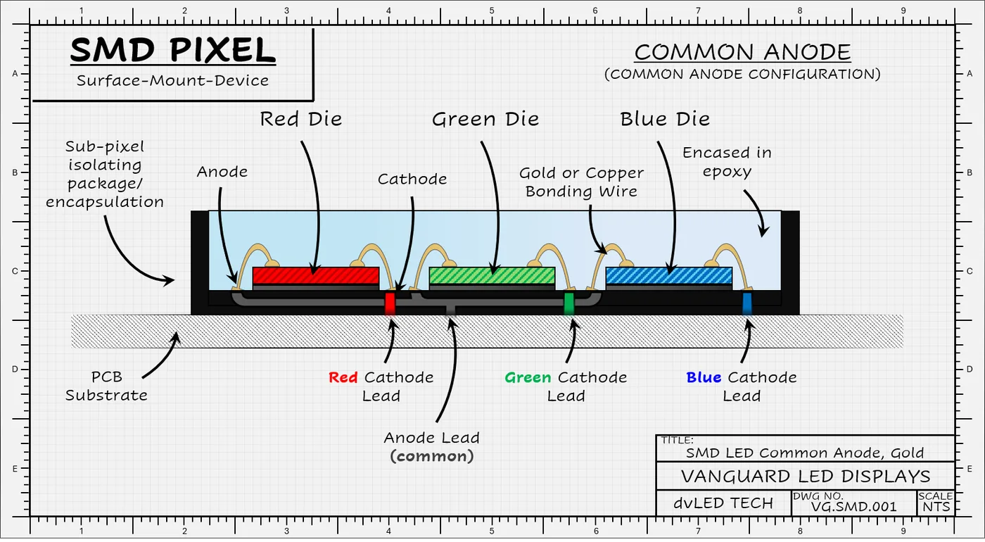
Surface-Mount Device (SMD) is the foundational pixel packaging technology of dvLED displays. Each SMD package encapsulates one red, one green, and one blue LED chip — wire-bonded into a small plastic or ceramic reflector cup — and is mechanically soldered directly to the PCB. SMD represents the most mature and widely deployed pixel technology in the industry, and is the architecture from which subsequent pixel technologies have evolved.
Quick reference
Term
Definition
SMD
A pixel package containing red, green, and blue LED chips wire-bonded into a reflector cup and soldered to a PCB
Reflector Cup
The plastic or ceramic housing that contains and optically isolates the RGB chips
Pixel Pitch
The distance in millimeters between the centers of two adjacent pixels
Binning
The process of sorting individual LED packages by wavelength and intensity before PCB mounting
Optical Isolation
The physical separation of pixels that preserves individual color integrity
PPM
Parts per million — the standard unit for measuring pixel failure rates
How SMD Works
An SMD pixel is a self-contained package. Three LED chips — red, green, and blue — are wire-bonded into a reflector cup and encapsulated with a protective resin. The completed package is then soldered onto the PCB using a mechanical pick-and-place process. The physical walls of the reflector cup provide optical isolation between pixels, ensuring that each pixel's color output remains discrete and uncontaminated by its neighbors.
This pixel-level encapsulation is a defining characteristic of SMD — and one it shares with MIP and IMD. It directly enables the color integrity, saturation, and depth that encapsulated pixel technologies achieve, and that COB — with its continuous flood coat encapsulation — cannot replicate.
SMD Pixel Pitch
The smallest achievable pixel pitch with SMD is P0.9. Below this threshold, the physical footprint of the SMD package and its solder pads exhausts the available PCB real estate. SMD is primarily deployed in indoor applications ranging from P0.9 to P2.5 and beyond.
Color Performance of SMD Pixels
Because each SMD pixel is individually encapsulated, its color output is optically isolated from adjacent pixels. This preserves color integrity at the pixel level — producing sharp, deep, and saturated color that continuous encapsulation technologies cannot match.
Prior to PCB mounting, individual SMD packages are tested, sorted, and binned by wavelength and intensity. This ensures exceptional color uniformity across the display with minimal reliance on software calibration.
Failure Rate of SMD Pixels
The estimated failure rate for SMD displays is 50–100 PPM in year one.
SMD Pixel Repair
All dvLED pixel failures result in a module swap in the field — a pulled module is replaced from spare stock and sent offsite for repair. For SMD and other encapsulated pixel technologies, offsite repair is performed at the pixel level — a relatively fast and lower-cost process. COB, by contrast, requires chip-level repair offsite, which takes longer and costs more.
Advantages of SMD
Color integrity — pixel-level encapsulation ensures discrete, isolated color output per pixel
Color uniformity — individual binning before mounting produces consistent results across the display
Maturity — the most established pixel technology in the industry, with highly optimized manufacturing yields
Cost efficiency — at pixel pitches above 1.5mm, SMD offers the lowest production cost of any pixel technology
Disadvantages of SMD
Pixel pitch floor — 0.9mm is the physical limit; finer pitches require a different pixel architecture
Impact vulnerability — exposed packages with multiple solder points are susceptible to physical displacement
Thermal management — heat must travel through wire bonds, package leads, and solder joints before reaching the PCB, creating multi-layer thermal resistance
Contrast — exposed package surfaces and solder leads reflect ambient light, lifting black levels and reducing contrast ratio
Pixels
Chip-On-Board (COB)
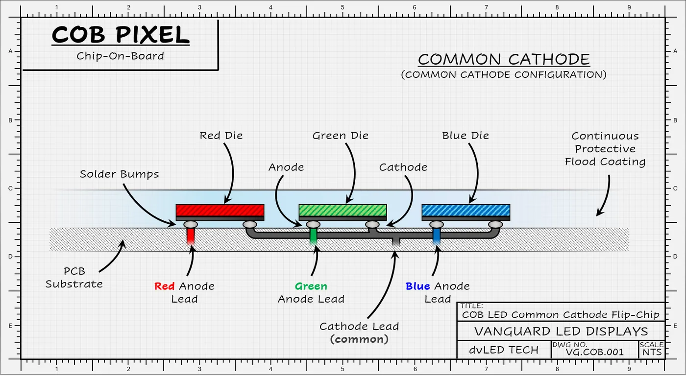
Chip-On-Board (COB) is a pixel packaging approach that removes the individual LED package entirely. Rather than soldering pre-packaged SMD pixels onto a PCB, COB mounts bare red, green, and blue LED chips directly onto the board, then covers the entire surface with a continuous flood coat of protective epoxy or silicone resin. COB has become increasingly common as manufacturing costs have dropped below SMD, making it an attractive option for price-sensitive deployments — though cost reduction is the primary driver of its adoption, not performance superiority.
Quick reference
Term
Definition
COB
A pixel architecture where bare LED chips are mounted directly to the PCB and covered with a continuous resin flood coat
Flood Coat
The continuous layer of epoxy or silicone resin that encapsulates the entire COB module surface
Sub-pixel Crosstalk
Light bleed between adjacent color channels caused by continuous encapsulation, softening color distinction
Dye Lot
A production batch of semiconductor material; chips from different dye lots exhibit slight color variations
Wire-Bonded COB
A legacy COB architecture using gold or copper wires to connect chips to the PCB
Flip-Chip COB
The current standard COB architecture using direct solder contact — no bond wires
How COB Works
Bare LED chips are placed directly onto the PCB substrate and electrically connected — either via wire bonding or flip-chip bonding. Once all chips are mounted and connected, the entire module surface is covered with a continuous resin flood coat that encapsulates all chips uniformly. There are no individual pixel housings or reflector cups.
COB Pixel Pitch
Without the physical constraints of an individual package, COB can achieve pixel pitches well below P0.9 — down to P0.4 and finer. This makes COB viable for high-resolution applications on smaller screen surfaces where SMD physically cannot go.
Color Performance for COB Pixels
COB's continuous flood coat presents color consistency challenges that pixel-level encapsulation avoids. Without physical walls isolating each pixel, light from adjacent color channels can intermingle — a phenomenon known as sub-pixel crosstalk. The result is a softening of color distinction that is difficult to fully correct through calibration.
Color uniformity is further complicated by dye lot variation. Because COB modules are populated with chips drawn from multiple production batches, slight color differences between dye lots can produce visible inconsistencies across the display surface. Sophisticated pixel-to-pixel calibration is required to compensate, though it cannot entirely eliminate the underlying variation.
Epoxy-treated SMD, MIP, and IMD retain pixel-level encapsulation while gaining comparable surface protection — achieving color performance that COB's continuous flood coat architecture cannot replicate.
Durability of COB pixels
COB's continuous resin surface is a genuine structural advantage. With no exposed individual packages or solder points, COB modules are resistant to dust, moisture, and physical impact at fine pixel pitches where non-epoxy SMD packages are most vulnerable.
Epoxy-treated SMD, MIP, and IMD can achieve comparable surface durability while retaining the structural and optical benefits of individual pixel encapsulation.
Thermal Management for COB pixels
Mounting chips directly to the PCB shortens the thermal path compared to wire-bonded SMD. Heat moves away from the die more directly, contributing to better longevity and color stability over sustained operation.
Repair of COB Chips
All dvLED pixel failures are initially resolved with a module swap in the field using spare modules included with the display. For COB, offsite repair requires chip-level intervention — a more intensive process than pixel-level repair available to encapsulated pixel technologies (SMD, IMD, MIP). COB module repair takes longer and costs more.
Advantages of COB
Fine pixel pitch — achievable below P0.9, enabling high-resolution configurations on smaller surfaces
Thermal efficiency — shorter thermal path from die to PCB compared to wire-bonded SMD
Contrast — full black resin flood coat produces deep black levels and wide viewing angles with no package walls or solder leads reflecting ambient light
Manufacturing cost — currently less expensive to produce than SMD at comparable pixel pitches
Disadvantages of COB
Color performance — continuous encapsulation introduces sub-pixel crosstalk and dye lot consistency challenges that pixel-level encapsulation avoids
Repair intensity — chip-level offsite repair is slower and more expensive than pixel-level repair
Calibration dependency — achieving acceptable color uniformity requires sophisticated calibration that encapsulated pixel technologies do not rely on as heavily
Pixels
Integrated-Matrix-Device (IMD)
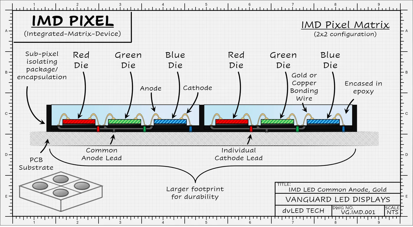
Integrated Matrix Device (IMD) is a pixel packaging format that groups multiple complete RGB pixels into a single mountable unit. The most common configuration is a 2x2 array — four fully independent pixels sharing one package footprint. IMD uses the same foundational pixel architecture as SMD, with each pixel maintaining its own reflector cup and individual encapsulation. The primary value of IMD is physical — a larger package footprint delivers meaningfully greater durability without requiring epoxy treatment.
Quick reference
Term
Definition
IMD
A pixel package containing a 2x2 array of complete, individually encapsulated RGB pixels
2x2 Array
The standard IMD configuration — four complete pixels per package
Package Footprint
The physical surface area of the mounted package and its solder contact points
Pixel Pitch
The distance in millimeters between the centers of two adjacent pixels
How IMD Works
An IMD package contains four complete RGB pixels arranged in a 2x2 grid. Each pixel within the package has its own reflector cup and operates independently — identical in function to a standalone SMD pixel. The bonding method within the package — gold wire, copper wire, or flip-chip — varies by manufacturer and is not indicated by the IMD format itself.
The completed package is mounted to the PCB using the same mechanical pick-and-place process as SMD, and is compatible with standard SMT manufacturing lines.
Pixel Pitch range for IMD
IMD is practical across a pixel pitch range of approximately P0.9 to P2.8. Below P0.9, the 2x2 package footprint becomes a constraint. Above P2.8, standard SMD is typically the more cost-effective choice.
Color Performance of IMD Pixels
Because each pixel within an IMD package has its own reflector cup, IMD shares the same color integrity characteristics as SMD. Pixel-level encapsulation prevents sub-pixel crosstalk, preserving sharp, saturated color output. Individual binning before mounting ensures color uniformity across the display.
Durability of IMD Pixels
IMD's defining advantage is physical durability derived from its larger package footprint. A greater solder contact area produces a more stable mechanical mount — making IMD significantly more resistant to physical displacement than SMD at comparable pixel pitches. As a reference point, a P1.2 IMD display will achieve durability comparable to a P2.5 SMD display without any epoxy treatment.
Epoxy treatment can be applied to IMD modules for additional surface protection, as with SMD and MIP.
Repair of IMD Pixels
All dvLED pixel failures result in a module swap in the field. For IMD, offsite repair is performed at the pixel level — the same process as SMD — making it relatively fast and cost-effective.
Advantages of IMD
Durability without epoxy — larger footprint provides structural stability equivalent to a display twice the pixel pitch
Color integrity — individual pixel encapsulation preserves color performance equivalent to SMD
SMT compatibility — mounts on standard pick-and-place lines, no specialized manufacturing required
Pitch range — covers P0.9 to P2.8, overlapping with both fine-pitch SMD and coarser deployments
Cost — at equivalent pitch, IMD carries a modest cost premium over SMD due to the more complex package
Array flexibility — alternative configurations beyond 2x2 exist but carry higher cost and limited industry traction
Pixels
Micro-In-Package (MIP)
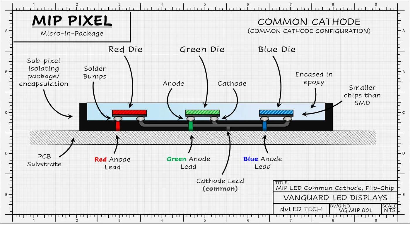
Micro-In-Package (MIP) is the natural evolution of SMD pixel technology scaled to ultra-fine pixel pitches. Rather than placing raw chips directly onto the display PCB, MIP fabricates complete, individually tested RGB pixel packages at a microscopic scale — then mounts them using standard SMT pick-and-place equipment. For this encyclopedia, MIP is defined as flip-chip bonded with common cathode power architecture, requiring compatible IC drivers to realize its efficiency advantages.
Quick reference
Term
Definition
MIP
An ultra-small, fully packaged RGB pixel using flip-chip bonding and common cathode architecture
Epitaxial Wafer
A semiconductor wafer with grown layers that determine LED color and efficiency
Interposer
A miniature carrier substrate onto which MIP chips are transferred and packaged
Singulation
The process of dicing a populated carrier substrate into individual MIP packages
Mura Effect
Color clouding or patchiness caused by inconsistent chip sorting across a display
SMT Compatibility
The ability to mount components using standard pick-and-place manufacturing lines
Common Cathode
A power architecture requiring both compatible pixels and compatible IC drivers
How MIP Works
MIP fabrication occurs in two distinct phases:
Phase 1 — Package Fabrication
RGB epitaxial wafers are diced into microscopic chips — typically 50–80 micrometers per side, compared to 200–300 micrometers for standard SMD dies. These chips are transferred onto a miniature interposer, flip-chip bonded directly to the interposer contacts, and encapsulated with epoxy or silicone resin. The populated carrier is then singulated into individual, fully functional RGB pixel packages.
Phase 2 — Panel Assembly
Because a MIP package presents standard contact pads on its underside, it can be tested, binned, and reeled exactly like an SMD component. Display manufacturers mount MIP packages onto the display PCB using existing high-speed SMT pick-and-place equipment — no specialized mass-transfer infrastructure required.
Color Performance in MIP Pixels
MIP packages are fully tested and optically binned before PCB mounting. This eliminates the mura effect — the color clouding or patchiness that results from inconsistent chip sorting — and produces exceptional color uniformity across the display without heavy reliance on software calibration.
Each MIP package maintains individual pixel encapsulation, preserving the color integrity and sub-pixel isolation that continuous encapsulation technologies cannot achieve.
MIP Pixel Pitch
MIP's microscopic chip scale enables pixel pitches below P0.9 — the physical limit of standard SMD — while retaining the manufacturing and testing advantages of packaged pixel technology.
Common Cathode and Flip-Chip in MIP Pixels
MIP as defined here uses flip-chip bonding within the package and common cathode power architecture at the system level. Common cathode requires a compatible handshake between the MIP pixel package and compatible IC drivers — both are necessary for the power efficiency advantages of common cathode to be realized. This combination eliminates wire bond failure points, maximizes light output, and significantly reduces heat generation and power consumption compared to wire-bonded, common anode alternatives.
MIP Pixel Repair
All dvLED pixel failures result in a module swap in the field. For MIP, offsite repair is performed at the pixel level — the same process as SMD and IMD — making it relatively fast and cost-effective.
Pre-mount testing and binning — eliminates yield risk and ensures color uniformity before PCB assembly
Color integrity — individual pixel encapsulation preserves sub-pixel isolation
SMT compatibility — mounts on existing pick-and-place lines, no new manufacturing infrastructure required
Thermal and reliability performance — flip-chip bonding eliminates wire failure points and shortens thermal path
Disadvantages of MIP
Cost — microscopic fabrication and precision packaging carries a higher per-pixel cost than SMD or IMD at equivalent pitches
IC driver dependency — common cathode efficiency requires compatible IC drivers; system-level compatibility must be verified
Pixels
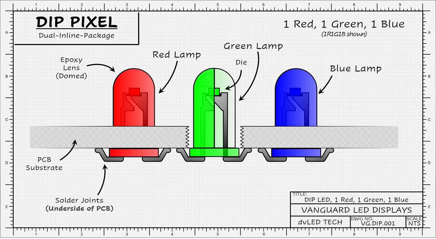
Dual-Inline-Packages (DIP)
Dual-Inline Package (DIP) is the original LED pixel technology — predating surface-mount architectures entirely. DIP LEDs are recognizable by their distinctive bullet-shaped epoxy lens and through-hole pin mounting. While largely superseded by SMD and its descendants for indoor applications, DIP remains the standard for large-scale outdoor installations where extreme brightness, weather resistance, and long viewing distances are the primary requirements.
Quick reference
Term
Definition
DIP
A through-hole LED package with a domed epoxy lens and two parallel metal pins inserted through the PCB
Through-hole Mounting
A mounting method where component pins pass through drilled PCB holes and are soldered from the reverse side
Epoxy Lens
The hard, domed resin shell that protects the LED die and directs light output
Lead Frame
The metal frame inside the package that supports the die and extends into the mounting pins
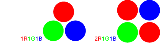
Pixel Cluster
The grouping of individual red, green, and blue DIP lamps that together form a single pixel
1R1G1B
A pixel cluster configuration using one red, one green, and one blue DIP lamp
2R1G1B
A pixel cluster configuration using two red lamps with one green and one blue — used where additional red output is needed
How DIP Works
A DIP LED is a single-color lamp. Each package contains one LED die — red, green, or blue — mounted on a lead frame inside a hard domed epoxy lens. Two parallel metal pins extend from the base of the package and are inserted through pre-drilled holes in the PCB, then soldered from the reverse side. This through-hole mounting method creates an exceptionally secure mechanical and electrical bond.
Unlike SMD and its descendants — where red, green, and blue chips are contained within a single package — a DIP pixel is formed by clustering individual lamps together on the board. The most common configurations are 1R1G1B and 2R1G1B. At typical DIP viewing distances, the light from the separate lamps blends to produce a full color image.
DIP Pixel Pitch
DIP's physical footprint and through-hole spacing produce pixel pitches typically ranging from P10 to P20 and above. This makes DIP unsuitable for close viewing but well matched to applications where the audience is measured in dozens of yards rather than feet.
Brightness of DIP Pixels
DIP LEDs are highly efficient at projecting light forward, routinely achieving 6,000 to 10,000+ nits. This makes DIP displays legible under direct sunlight — a threshold that indoor pixel technologies are not designed to meet.
Durability and Weather Resistance
The thick epoxy lens provides robust physical protection against impact, debris, and environmental exposure. DIP displays are highly receptive to conformal coatings, routinely achieving IP65 or IP67 ratings. The raised physical profile of the lens also promotes passive heat dissipation into surrounding air, contributing to long operational lifespan in demanding outdoor environments.
Repair of DIP pixels
All dvLED pixel failures follow the same field workflow — module swap from onsite spares, with the removed module sent offsite for repair. DIP is the most straightforward pixel technology to repair. The large physical scale of individual lamps makes component access and replacement significantly easier than any surface-mount or chip-level technology. By comparison, encapsulated pixel technologies (SMD, IMD, MIP) require pixel-level repair, and COB requires chip-level intervention — the most intensive and costly repair process across all pixel technologies.
Advantages of DIP
Extreme brightness — 6,000 to 10,000+ nits, suitable for direct sunlight viewing
Weather resistance — thick epoxy lens and conformal coating compatibility produce robust IP ratings
Mechanical durability — through-hole mounting is the most physically secure PCB attachment method of any pixel technology
Repairability — large component scale makes offsite repair the simplest of all pixel technologies
Manufacturing complexity — through-hole assembly is more labor-intensive than SMT, contributing to higher production costs
Resolution — large pixel pitch limits achievable resolution at any given screen size
Components
Modules
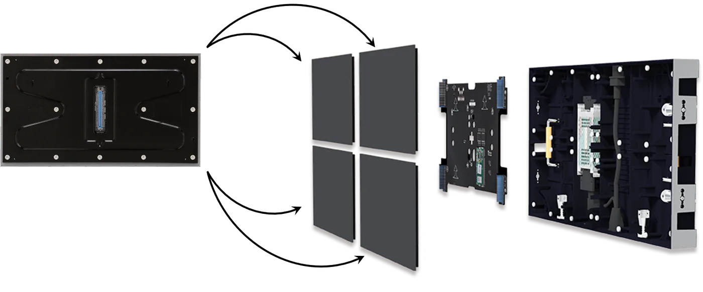
A module is the fundamental building block of a dvLED panel. It is a self-contained assembly that carries the pixels, the electronics that drive them, and the means to attach to the panel frame. Modules are designed to be swapped quickly in the field, making them the primary unit of both installation and maintenance. Spare modules, which are included in the original display sale, are factory calibrated with all modules at the same time to establish global color uniformity and hot swapping of spare modules without special tuning.
Sometimes being referred to as an LDM (LED Display Module), "module" is the most used term for the component.
Quick reference
Term
Definition
Module
A self-contained LED display assembly containing pixels, IC drivers, and mounting hardware
LDM
LED Display Module — an alternate term for module, less preferred due to unnecessary complexity
Panel
The complete display unit — metal frame, modules, HUB board, receiving card, and power supply. Also called a tile or cabinet; though panel is most common
PCB
Printed Circuit Board — the substrate that carries and connects all module components
IC Driver
Integrated circuit that controls pixel grayscale and refresh rate
Thermal Via
A copper-plated hole in the PCB that transfers heat from the front surface to the rear of the module
Ghost-Cancelling Circuit
Specialized PCB traces and components that prevent faint illumination of pixels that should be off
Flash Memory
Optional onboard storage for module-level calibration data
What a Module Contains
A module consists of:
Pixels — SMD, IMD, MIP, COB, or DIP, depending on the display technology
A PCB — the substrate that physically supports the pixels and hosts all driving electronics
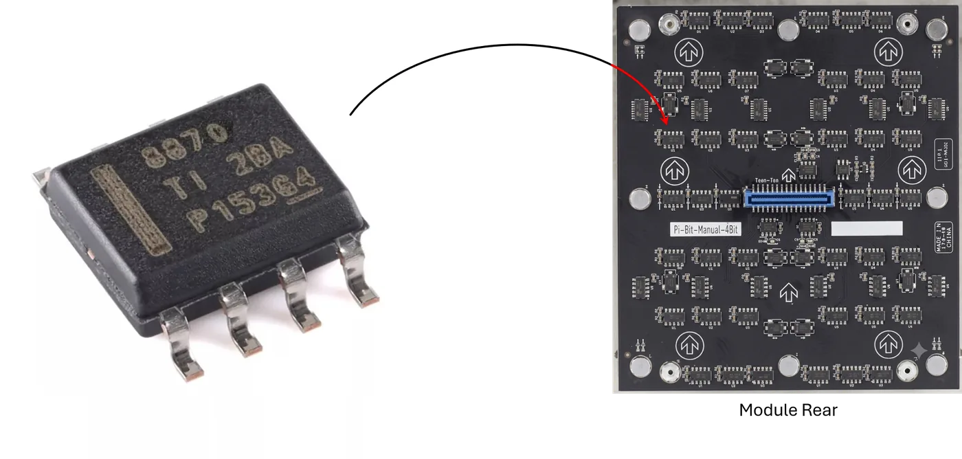
IC Drivers — integrated circuits soldered to the PCB that receive signal data and tell each red, green, and blue sub-pixel when to illuminate and at what intensity
Ghost-canceling circuits — specialized traces and components that prevent pixels from faintly illuminating when they should be fully off
Magnets — the primary method of securing modules to the panel frame; outdoor modules typically include locking mechanisms, with screw fastening available in some outdoor configurations
Flash memory(optional) — some modules store their own calibration data locally, allowing module-level calibration independent of central display calibration
The Module PCB
The module PCB is the structural and electrical foundation of the module. In a dvLED module, the module’s PCB performs several specialized functions beyond simple component connection:
Structural Mounting
Module PCBs provides the precision substrate onto which pixels are mounted. Pixel pitch consistency depends on PCB manufacturing accuracy — even minor warping or misalignment can produce visible seams or dark lines across the display surface.
Electrical Routing and Signal Distribution
The module PCB is a multi-layer circuit that routes high-speed signals from the HUB board to the IC drivers. High-end module PCBs use 6 to 10 layers to separate data signals from power traces, minimizing electromagnetic interference. Most modules pass signal data through directly from the HUB board; processing occurs upstream.
Thermal Management
Heat generated by the pixels travels through thermal vias — small copper-plated holes in the PCB — moving heat away from the front pixel surface toward the rear of the module and into the panel frame.
Power Distribution
The module receives DC power from the HUB board and distributes it across the module. This PCB design minimizes voltage drop to ensure consistent brightness from edge to edge.
How Modules Relate to Panels
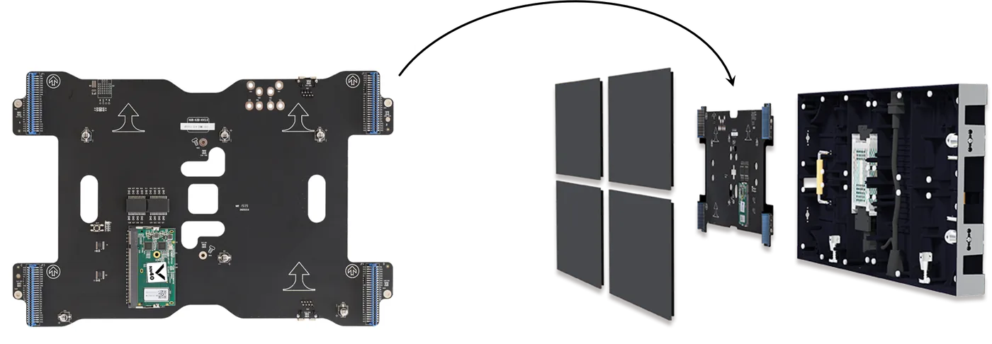
A panel is the complete display unit — metal frame, modules, HUB board, receiving card, and power supply. The number of modules per panel varies depending on module size and panel dimensions. A common indoor module size for 16:9 compatible display series is 300 x 168.75mm.
Power originates from the power supply housed within the panel and is passed to modules through the HUB board. The HUB board distributes both power and data to each module. These components are covered in detail in their respective articles.
Calibration
A dvLED display can operate from central calibration managed at the receiving card level, or from module-level calibration where individual modules store their own calibration data in onboard flash memory. Module-level calibration allows a replaced module to match the brightness and color of surrounding modules without recalibrating the entire display.
Repair
All dvLED pixel failures follow the same field workflow — a module is swapped from onsite spares and the pulled module is sent offsite for repair. The repairability of the module itself depends on the pixel technology it carries. DIP is the most straightforward to repair at the component level; encapsulated pixel technologies (SMD, IMD, MIP) require pixel-level repair; COB requires chip-level intervention, the most intensive and costly repair process.
Components
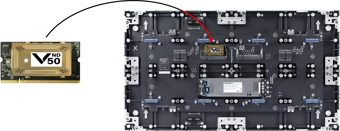
Receiving Cards
A receiving card is a small PCB mounted inside each dvLED panel that translates incoming video signal data into precise pixel-level instructions for every module in that panel. Where a video controller or sending card manages the overall display, the receiving card is responsible for its individual panel — decoding the signal, distributing data to modules, managing calibration, and controlling refresh behavior. It is one side of a signal handshake with the sending card, which is covered in a separate article.
Quick reference
Term
Definition
Receiving Card
A PCB inside each panel that decodes incoming video data and distributes pixel instructions to modules via the HUB board
Sending Card
The upstream signal source that feeds data to receiving cards across the display
Loading Capacity
The maximum number of pixels a single receiving card can control
Grayscale Depth
The number of discrete brightness levels a card can resolve per color channel, expressed in bits
Refresh Rate
The number of times per second the display updates its image, measured in Hz
Redundancy
The ability to maintain signal if a primary connection fails
Cascading
A signal topology where data passes from one receiving card to the next in sequence. A cascading is also commonly referred to as a ‘daisy-chain’
TAA Compliant
Trade Agreements Act compliant — a requirement for display hardware used in US federal government installations
Core Functions
Signal Decoding
The receiving card accepts a high-speed data stream — typically via Ethernet — from the sending card or video controller and decodes it into instructions the IC drivers on each module can execute.
Data Distribution
Decoded pixel data is routed through the HUB board to the correct modules within the panel. Each module receives only the instructions relevant to its pixel coordinates.
Image Processing and Calibration
The receiving card manages grayscale levels, color calibration, and brightness uniformity across all modules in its panel. Calibration coefficients are stored on the card, allowing a replaced module to be matched to surrounding panels without full recalibration.
Scanning and Refresh Control
The receiving card controls the refresh rate and scan timing of the LEDs — preventing visible flicker and ensuring stable image capture on camera, which is critical for broadcast and virtual production applications.
Signal Topology
Receiving cards support cascading — a signal topology where data enters the first panel's receiving card, and the remaining signal is passed downstream to the next card in sequence. This allows a single signal source to drive multiple panels across a large installation without requiring a dedicated connection to each panel individually.
Loading Capacity
Loading capacity defines how many pixels a single receiving card can drive. Cards in current production typically handle loading capacities ranging from 512×384 to 768×432 pixels per card, with data group configurations of 32. Higher-end installations may require cards with greater capacity or multiple cards per panel.
Grayscale and HDR
Entry-level receiving cards support 8-bit grayscale processing. Mid-range and high-end cards support 10-bit and 12-bit processing, enabling HDR content playback and smooth gradients without visible banding. Cards intended for high-end applications should support 12-bit processing at minimum.
Refresh Rate
Receiving cards support refresh rates ranging from 30Hz on basic configurations to 240Hz on higher-end cards. Higher refresh rates are essential for camera-facing applications where low refresh rates produce visible scan lines in captured footage.
Redundancy
Quality receiving cards support signal loop redundancy — if a primary signal cable fails, the card switches to a backup signal path automatically, preventing the panel from going dark. Dual card redundancy options are available for mission-critical installations.
Transmission
Current receiving cards operate at 1G transmission rates over standard Ethernet, with next-generation fiber-based receiving cards supporting 5Gb/s transmission rates and maximum transmission distances of up to 2km — an emerging option suited to large-scale and distributed installations.
Receiving Card Manufacturers
Receiving cards are produced by a small number of companies that dominate the market. Vanguard receiving cards are TAA compliant, making them suitable for US federal government installations. Other widely used manufacturers include:
NovaStar
Colorlight
Brompton Technology — widely used in high-end film and virtual production applications
Components
HUB Boards
A HUB board is a PCB mounted inside each dvLED panel that serves as the distribution hub between the receiving card, power supply and the individual modules. It has no processing role — its function is routing. The receiving card handles signal decoding; the HUB board takes the output of that process and delivers both low-voltage DC power and data to every module in the panel. Sometimes referred to as an Interface Board, HUB board is the most common term.
Quick reference
Term
Definition
HUB Board
A PCB inside each panel that routes power and data from the receiving card to individual modules
Interface Board
An alternate term for HUB board
RGB Data
Pixel-level color and brightness instructions routed to each module
Clock and Latch Signals
Timing signals that tell IC drivers when to refresh pixels
Scan/Address Lines
Signals that control which rows of the LED matrix are active at any given moment
Multi-layer PCB
A circuit board with multiple internal layers separating power and data traces to reduce electromagnetic interference
Ribbon Cable
A flat flexible cable used to connect HUB boards to modules in traditional panel architectures
Pinless Connection
A board-to-board pin header connection where modules plug directly into the HUB board — no cables required
Telemetry
Real-time monitoring data reported by the HUB board to the control system
HUB Board PCB Construction
Like the module PCB, the HUB board is itself a printed circuit board, manufactured to the same standards of precision required throughout an LED panel. Structural accuracy matters here as much as it does on the module — the HUB board's connectors must align precisely with both the receiving card above it and the modules it serves, since even minor manufacturing tolerance issues can produce signal or power delivery problems across the panel.
HUB boards are typically multi-layer PCBs, separating power traces from data and signal traces to minimize electromagnetic interference — the same layering principle applied to module PCBs, scaled to the HUB board's higher current-carrying requirements as the panel's central power and data distribution point.
What a HUB Board Does
Data Distribution
The receiving card connects to the HUB board via high-density board-to-board connectors. The HUB board then routes three categories of signals to each module:
RGB Data — pixel-level color and brightness instructions
Clock and Latch Signals — timing signals that synchronize IC driver refresh cycles
Scan/Address Lines — signals that control which rows of the pixel matrix are active at each moment, critical for scan-drive displays
Power Distribution
The HUB board receives low-voltage DC power from the panel's power supply and distributes it to each module. Power is routed cleanly across the board to maintain stable voltage from module to module — preventing brightness variation or flicker caused by voltage drop.
Calibration Support
The HUB board facilitates calibration data management between the receiving card and individual modules. When a module is replaced, the HUB board assists in applying stored calibration coefficients to the new module, ensuring it matches the brightness and color of surrounding modules. Calibration storage is covered in detail in the Modules and Receiving Cards articles.
Telemetry and Monitoring
HUB boards in commercial and rental panels typically integrate monitoring circuitry that tracks and reports real-time data to the control system, including:
Module and cabinet temperature
Humidity levels inside the panel chassis
Voltage stability across the board
Cable and module connection integrity — detecting unseated modules, open circuits, or short circuits
Connection Architecture
HUB board designs fall into two categories based on how they connect to modules:
Ribbon Cable (Legacy)
The HUB board sits centrally within the panel and connects to modules via flat ribbon cables — typically using HUB75 or HUB320 interface standards. This architecture is common in rental and staging panels where frequent module access and fast swaps are a priority.
Pinless / Board-to-Board (Modern Standard)
Modules plug directly into the HUB board via rigid gold-plated pin headers, eliminating cables entirely. This architecture is standard in fine-pitch displays at sub-1.5mm pixel pitch, where cable routing introduces alignment risk and potential signal degradation.
Components
Integrated Circuits (IC Drivers)
Integrated Circuit (IC) drivers are the execution layer of a dvLED display. Mounted directly on each module's PCB, they receive decoded pixel instructions from the receiving card via the HUB board and translate them into the precise electrical currents needed to illuminate each red, green, and blue sub-pixel at the correct brightness. Every pixel on every module is under the direct control of an IC driver.
The quality of the IC driver is one of the primary factors separating standard commercial displays from broadcast-grade and virtual production installations.
Quick reference
Term
Definition
IC Driver
An integrated circuit on the module PCB that controls pixel illumination by regulating current and managing timing
Constant Current Drive
A regulation method that delivers a stable, fixed current to each LED regardless of voltage fluctuations
PWM
Pulse Width Modulation — a technique that controls perceived brightness by rapidly switching LEDs on and off
Duty Cycle
The ratio of on-time to off-time within a PWM cycle — determines perceived brightness level
Grayscale Depth
The number of discrete brightness levels per color channel, expressed in bits
Multiplexing
A technique where IC drivers illuminate one row of pixels at a time in rapid sequence, creating the perception of a fully lit display
Scan Rate
The rate at which rows are cycled through during multiplexing, expressed as a fraction (e.g., 1/16, 1/32)
Ghosting
Faint illumination of pixels that should be off, caused by residual charge in the circuit
Caterpillar Effect
A fault condition where a shorted LED causes an entire row or column to illuminate incorrectly
HDR
High Dynamic Range — content requiring simultaneous high peak brightness and fine shadow detail
Constant Current Regulation
LEDs are current-driven devices — their brightness is determined by the amount of current flowing through them, not voltage. Small voltage fluctuations can produce significant brightness variation or damage the die. IC drivers use constant current drive technology to deliver a stable, fixed current to every pixel regardless of fluctuations in the power supply or operating temperature. This prevents the patchy, uneven brightness that results from unregulated current delivery.
Grayscale and Color Depth — PWM
To display full-color video, each sub-pixel must be capable of producing thousands of distinct brightness levels. IC drivers achieve this through Pulse Width Modulation — rapidly switching each LED on and off within a fraction of a millisecond. The ratio of on-time to off-time within each cycle is the duty cycle, and it is this ratio that determines perceived brightness. The human eye integrates the rapid switching as a continuous level of light.
High-end IC drivers achieve 14-bit to 16-bit grayscale depth, enabling smooth gradients, accurate shadow detail, and HDR content reproduction without visible color banding.
IC Drivers are the original Flip-Chip
Integrated circuit drivers were among the first semiconductor components to be mounted using wire bonding — a technique dating to the early 1960s, when fine gold wires were used to connect the top-facing contact pads of IC chips to their surrounding lead frames. The same approach was later adopted for LED die mounting in dvLED displays, connecting the anode and cathode pads of each die to the lead frame via gold or copper bond wires.
In 1964, IBM pioneered the first flip-chip IC mounting process — inverting the chip so its contact pads faced downward and connected directly to the substrate via solder bumps, eliminating bond wires entirely. The advantages were immediate: shorter electrical paths, better thermal management, higher reliability, and the ability to pack components more densely. Flip-chip became the standard mounting method for high-performance IC drivers long before the dvLED industry existed.
LED pixel mounting technology is now following the same evolutionary path. Wire-bonded SMD pixels — the direct analog of early wire-bonded IC mounting — are giving way to flip-chip bonded pixels in MIP and COB architectures, driven by the same engineering imperatives that pushed IC drivers toward flip-chip decades earlier. The dvLED industry is not inventing a new technology so much as applying a proven one to a new component.
Multiplexing and Scan Rate
Providing a dedicated continuous signal to every LED on a module would require an impractical number of PCB connections, particularly at fine pixel pitches. IC drivers manage this through multiplexing — illuminating one row of pixels at a time and cycling through all rows fast enough that the human eye perceives a fully and simultaneously lit display.
Scan rate describes how this cycling is divided — expressed as fractions like 1/16, 1/32, or 1/64. Advanced IC drivers optimize multiplexing timing to maintain a stable, flicker-free image even under high-speed broadcast camera capture.
Image Quality and Artifact Management
Ghosting Elimination
When IC drivers switch rapidly between rows, residual charge remaining in the circuit can cause pixels to glow faintly when they should be fully off — a condition called ghosting. IC drivers include blanking circuits that actively discharge residual electricity between row cycles, ensuring deep blacks and clean pixel edges.
Caterpillar Effect Mitigation
If a single LED develops a short circuit, it can cause an entire row or column to illuminate incorrectly — a fault pattern referred to as the caterpillar effect. Advanced IC drivers isolate the affected pixel electrically, preventing the fault from propagating to neighboring diodes.
Error Detection
Many IC drivers monitor for open and short circuit conditions across the pixel matrix, reporting the precise location of any detected fault back to the control system.
HDR Support
Modern IC drivers are designed to handle the simultaneous demands of HDR content — high peak brightness for highlights alongside fine gradation in shadow detail. Current gain management allows the display to boost brightness for bright image elements without losing detail in dark areas.
PWM Frequency and Display Grade
PWM frequency determines how many times per second each LED is switched on and off. Higher frequencies reduce the risk of visible flicker, particularly under camera capture. High-end IC drivers operate at PWM frequencies of 7,680Hz and above. This is one of the clearest technical distinctions between standard commercial IC drivers and those used in broadcast and virtual production displays.
Common Cathode Integration
IC drivers are one half of the common cathode handshake. For common cathode power architecture to function, both the pixel and the IC driver must support it. Compatible IC drivers enable the per-color voltage management that reduces heat and power consumption. This is covered in detail in the Common Cathode Technology article.
Components
Power Supplies
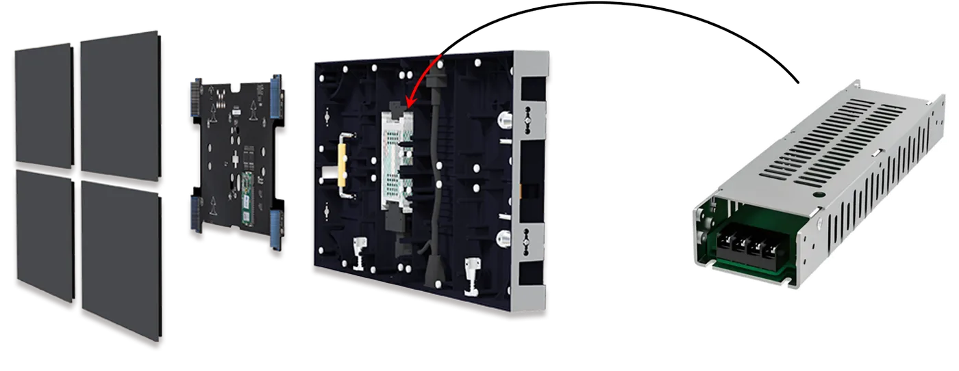
Every dvLED panel contains one or more Low Voltage Power Supplies (LVPS) that convert incoming AC power to the stable low-voltage DC required by the display's modules, HUB board, receiving card, and IC drivers. The LVPS is a dedicated internal component — not a general-purpose power supply — engineered to deliver clean, stable DC output under the continuous demands of a running display.
Quick reference
Term
Definition
LVPS
Low Voltage Power Supply — converts AC input to low-voltage DC output for panel components
AC Input
Alternating current from building power, typically 100–240V
DC Output
Direct current delivered to panel components at low voltage
Redundant Power
A configuration where two LVPS units share the panel load, allowing either to carry the full load if the other fails
Load Capacity
The maximum power draw a single LVPS can sustain
How the LVPS Works
The LVPS accepts standard AC building power — ranging from 100V to 240V to support high-voltage applications and international AC power standards — and converts it to stable low-voltage DC output in the range of 3.8V to 5V. This output is delivered directly to the HUB board, which distributes power to each module in the panel. The stability of this DC output is critical — fluctuations in voltage directly affect brightness consistency and IC driver performance across the display.
Panel Power Configuration
Depending on panel size and power requirements, a panel may contain a single LVPS or multiple units. Spare power supplies are included with every display purchase and require no calibration or configuration — they are direct replacements.
Redundancy
For installations where display continuity is critical, many panel series can be configured with redundant power supplies. In a redundant configuration, two LVPS units are both actively connected and share the panel load — each operating at less than half its rated capacity during normal operation. If one unit fails, the other automatically assumes the full load without any interruption to the display image.
This passive load-sharing approach means there is no failover delay and no image loss — the transition is instantaneous and invisible to the viewer.
Power Supply Replacement
Replacing an LVPS requires no special tools or calibration. The process is:
Disconnect incoming AC power — either at the circuit breaker or by disconnecting the AC cascade to the panel
Swap the failed unit with a spare
Restore AC power
The display resumes normal operation immediately. Spare LVPS units are included with every display and are interchangeable within compatible panel models.
Controllers
Controller/Processors
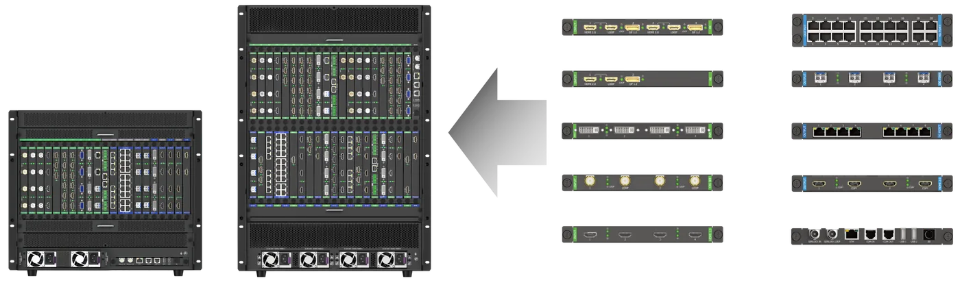
A controller (also called a ‘sender’, and at the high end, a ‘processor’) is the accessory that feeds video signal data to an LED display's receiving cards. If an LED display is thought of as a car, the sender is the engine: essential, constantly discussed, but not the subject most people are pointing at when they talk about "the display." The controller is the car. It accepts a video source, prepares that signal appropriately, and sends it downstream to the receiving cards across the display.
Not every controller processes the signal. Some simply pass pixels through unchanged — these are senders in the most literal sense. Controllers that scale, window, or otherwise manipulate the signal before sending it are commonly referred to as processors. Terminology across the industry is not rigidly standardized — "controller," "sender," and "processor" are often used interchangeably depending on the manufacturer and the person speaking. None of these usages are inherently incorrect.
Quick reference
Term
Definition
Controller
The umbrella term for any device that sends video signal to a dvLED display's receiving cards
Sender
The core function of a controller — transmitting signal downstream to receiving cards
Processor
A controller capable of scaling, windowing, or layout manipulation — a higher capability tier within the controller family
Bit Processing
The color bit depth (8-bit, 10-bit, 12-bit) at which a controller processes and transmits signal
Pixel Load (Port)
The maximum number of pixels a single controller output port can drive
Pixel Load (Controller)
The maximum number of pixels a controller can manage overall — governed by input capability, not simply the sum of output ports
Ecosystem Compatibility
The requirement that sender and receiving card come from the same manufacturer to function together
Bit Processing and Pixel Load
A controller's output capacity is tied directly to its processing bit depth. At standard 8-bit color processing, a single 1G output port can drive 655,360 pixels. As bit depth increases — to 10-bit or 12-bit, supporting HDR and finer gradation — the pixel load per port decreases, since more data is required per pixel at the same transmission rate.
Pixel load must be considered at two levels:
Per port — the maximum pixels a single output can carry to the LED display
Per controller — the maximum pixels the controller can receive from any individual input port
Critically, the per-controller ceiling is not simply the sum of all output ports' capacities. A controller's true limit is governed equally by both ends of the signal chain — its input capability and its output capability. Most controllers can only accept a source signal up to 2K or 4K resolution, regardless of how much pixel capacity their output ports could theoretically support. This becomes especially apparent with card-chassis systems, where total output capacity can far exceed what any single input is capable of feeding it. Controller selection requires matching both the source resolution being fed in and the total display pixel count being driven out.
Ecosystem Compatibility
Senders and receiving cards must come from the same manufacturer ecosystem to function together. A controller from one provider cannot be mixed with receiving cards from another — the signal protocol, calibration handshake, and data formatting are proprietary to each ecosystem. This is a critical consideration during system design, particularly when integrating an LED display into an existing AV environment built around a different controller brand.
Outputs
Controllers output signal in two broad categories:
To LED Displays: Ethernet and Fiber, at 1G or 5G transmission rates — the same transmission methods received by the dvLED display's Receiving Cards, covered in detail in that article.
To Other Display Technologies: HDMI and DVI, allowing a single controller to drive non-LED displays alongside or instead of a dvLED panel.
The Four Categories of Controllers
Pixel-to-Pixel
The most basic controller category — a true sender with no processing capability. Source content is mapped directly to display pixels on a 1:1 basis, with no scaling or fitting. This requires the source resolution to already match the display's native resolution. Pixel-to-pixel controllers are the simplest and most cost-effective option for fixed installations where content is pre-formatted to the exact resolution of the display. It is important to note that with Pixel-to-Pixel controllers, 2K and 4K sources cannot be scaled to the other’s resolution. If the LED display is 4K and a 2K source is connected, it will only fill a quarter of the LED display.
Scaling
A step up from pixel-to-pixel, scaling controllers can take a source of any resolution and fit or fill it to the display's actual resolution. This adds flexibility for installations where source content doesn't perfectly match display dimensions, without the cost or complexity of full processing capability.
Card-Chassis
The most capable and configurable controller category. Card-chassis systems are fully processing — supporting windowing, multiple simultaneous sources, configurable layouts, and scalability through a family of interchangeable input and output cards across multiple chassis sizes. Output support extends beyond dvLED to other display technologies via HDMI, DisplayPort, and other standards. Card-chassis processors are the standard choice for control rooms, command centers, and complex multi-source installations.
Media Player
Media player controllers include local flash storage, allowing content to be stored and played back directly from the controller without requiring a live, continuously connected source. This makes them well suited to standalone applications — retail signage, scheduled content, and installations where a persistent live feed isn't practical or necessary.
Source Feeding Methods
Controllers vary in how they accept and route source content:
Single-in, single-out — one source feeds one display output, the simplest configuration
Multiple-in, matrixed-out — multiple sources are received and routed, windowed, or layered onto a single display canvas — a capability associated with card-chassis processors. This type of controller is necessary when only one of its defined functions is needed. Multiple-in to a single view layout, and few sources for a windowed layout.
Broadcast and Camera Considerations
For displays used in broadcast or virtual production environments, controller selection must account for genlock and frame synchronization, color accuracy, and compatibility with camera-facing refresh rates. These considerations connect directly to the refresh rate and scan timing capabilities covered in the Receiving Cards and Integrated Circuits (IC Drivers) articles — the controller and the display's internal electronics must be aligned for stable, flicker-free camera capture.
Controllers
Advanced processing in Card-Chassis Controllers
Card-chassis processors represent the most configurable and capable category of dvLED controller. Rather than a fixed set of inputs and outputs, a card-chassis system is built around a modular rack-mounted frame that accepts interchangeable input and output cards — allowing each system to be configured precisely to the signal sources and display technologies it needs to support. This article focuses on the processing capabilities, windowing, card architecture, and redundancy features that define this category, building on the foundation covered in the Controller/Processors article.
Quick reference
Term
Definition
Chassis
The modular rack-mounted frame that houses input and output cards
RU (Rack Unit)
A standard unit of rack height; chassis sizes range from 2RU to 20RU depending on card capacity needed
Card Slot
A physical bay within the chassis that accepts a single input or output card
Window
An independently defined region of the display canvas, capable of showing its own source, size, and position
Z-Order (Layering)
The stacking order of windows, determining which window appears on top when overlapping
Copper Ethernet
Standard transmission method from controller to display, supporting cable runs up to 100m (328ft)
Fiber
Transmission method supporting distances up to 2km, used when copper's range is insufficient
Fiber Receiver
A device that converts a single fiber connection into multiple 1G Ethernet outputs for distribution to receiving cards. Fiber Receivers are typically located near the display.
Fiber Receiving Card
A receiving card which directly accepts 5G fiber from the Controller/Processor. Fiber Receiving Cards enable expanded configurations while using no copper in the data path.
SDI
Serial Digital Interface — a broadcast-standard video transmission format, available in 3G and 12G variants
NDI
Network Device Interface — an IP-based protocol for transmitting broadcast-quality video over standard network infrastructure
ST 2110
A broadcast industry standard for transmitting uncompressed video over IP networks
Chassis Sizing
Card-chassis systems are available in a range of physical sizes, from compact 2RU frames suited to smaller installations up to large 20RU frames supporting extensive multi-source, multi-display environments. Chassis size determines the number of available card slots — and therefore the upper bound of total input and output capacity the system can support. Selecting the right chassis size requires forecasting not just current needs but anticipated growth in source count and display complexity.
Card Architecture
A card-chassis system's flexibility comes from its modular card families, which fall into four functional groups:
Display I/O Cards
Standard consumer and commercial display connections — HDMI, DVI, and DisplayPort, in single and multi-port configurations, including high-bandwidth variants such as HDMI 2.0/2.1 and DisplayPort 1.2/1.4 that support higher resolutions and refresh rates.
Broadcast I/O Cards
SDI cards (3G-SDI and 12G-SDI) provide the signal format standard to broadcast and production environments. These cards are essential for any installation that must interface with broadcast camera systems, switchers, or production infrastructure.
Network I/O Cards
IP-based video transmission cards, including NDI and ST 2110, allow video to be sent and received over standard network infrastructure rather than dedicated video cabling. These formats are increasingly common in modern broadcast and virtual production workflows, where flexibility and distance are prioritized over traditional point-to-point cabling.
LED Output Cards
High-density Ethernet and Fiber output cards that feed the display's receiving cards directly, as covered in the Controller/Processors article. A single output card can carry many individual ports — output cards offering as many as 20 RJ45 1G ports on one card are common. This matters directly to total system capacity: a chassis's true output capability is the product of both card slot count and ports-per-card, not simply the number of physical card bays.
Transmission Distance to the Display
The transmission method connecting a controller's output to the display's receiving cards is governed primarily by distance.
Copper Ethernet is the standard connection method, supporting cable runs of up to 100 meters (328 feet). This covers the vast majority of installations where the controller is located reasonably close to the display.
Fiber is used when greater distance is required — supporting transmission up to 2 kilometers, making it suitable for large venues, distributed installations, or any scenario where the controller and display are separated beyond copper's practical limit.
If sending fiber to the LED display, there are options to use a Fiber Receiver which sits at the display end of a fiber run, converting a single 10G fiber connection into ten individual 1G Ethernet outputs — distributing the signal back into standard copper connections that feed the display's receiving cards directly. Fiber receiving cards are an emerging technology which enables sending 5G fiber directly into each panel. When using Fiber Receiving Cards, the pixel load increases allowing fewer cables run between the Controller/Processor and the LED panels.
Windowing and Layout
The defining processing capability of a card-chassis system is windowing — the ability to define multiple independent regions on the display canvas, each showing its own source content, at its own size and position. Windows can be freely resized, repositioned, and layered.
Z-order (layering) determines which window appears on top when two or more overlap — allowing, for example, a full-screen background source with a smaller picture-in-picture window layered above it.
This capability is what separates card-chassis processors from simpler scaling controllers. Where a scaling controller fits one source to the full display, a card-chassis processor can simultaneously manage many independent sources across a single canvas — common in command center and control room environments where multiple live feeds, maps, and data sources must be visible at once on a shared video wall.
Redundancy
All controllers support basic redundancy for the LED signal connection, as covered in the Controller/Processors article. Card-chassis systems extend this with additional redundancy options at the card level:
Backup-capable cards — certain input and output cards support a backup configuration, maintaining a secondary signal path that activates automatically if the primary connection fails
Loop-capable cards — certain cards support signal looping, allowing a single source to be passed through to additional downstream equipment without requiring a separate distribution device
These card-level redundancy features supplement the chassis's basic output redundancy, providing layered protection appropriate to mission-critical installations such as broadcast studios and command centers, where any signal interruption is unacceptable.
Use Cases
Card-chassis processors are the standard choice for environments demanding multi-source flexibility and broadcast-grade reliability:
Command and control centers — multiple live feeds, data sources, and maps displayed simultaneously across a shared video wall
Control rooms — operational monitoring environments requiring flexible, reconfigurable layouts as situations evolve
Broadcast and virtual production studios — environments requiring SDI, NDI, or ST 2110 compatibility alongside precise genlock and frame synchronization with camera systems